Mechanical tests followed by microstructural investigations provide engineers with information to computationally predict the mechanical performance of components. Electron microscopy is one of the most well-known techniques for analyzing deformation features of materials and understanding their response to external sollicitations. Two types of electron microscopes are commonly used and provide complementary information: Transmission Electron Microscopy (TEM) at the micro/nano-scale and Scanning Electron Microscopy (SEM) at the macro/mesoscopic scale.
Transmission Electron Microscope (TEM)
TEM is a renowned technique for observing and characterizing crystalline defects at both sub-micron and nanoscales in electron-transparent thin foils (approximately 100 nm thick). These comprehensive studies at the microscopic scale offer valuable insights for extrapolating to the macroscopic response of materials.
Scanning Electron Microscope (SEM)
Electromagnetic lenses focus the electron beam emitted by an electron gun onto the sample, causing the formation of new electrons through interaction. These electrons are then detected and converted into an electrical signal. This process is repeated for each point on the sample through scanning, enabling the reconstruction of the sample’s surface topography.
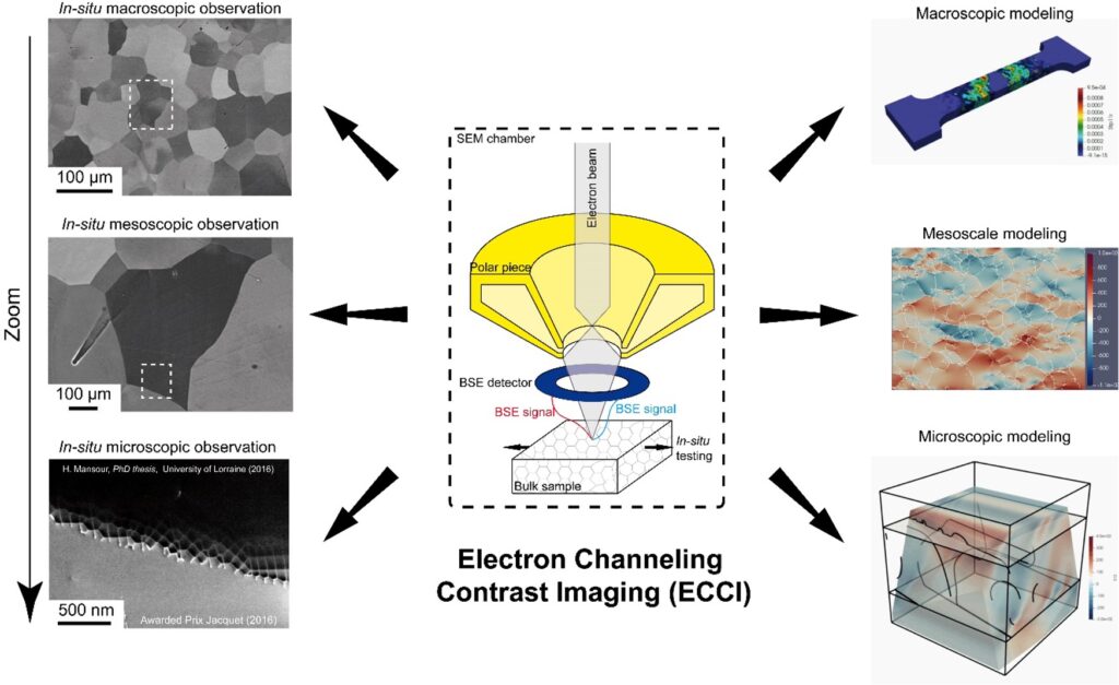
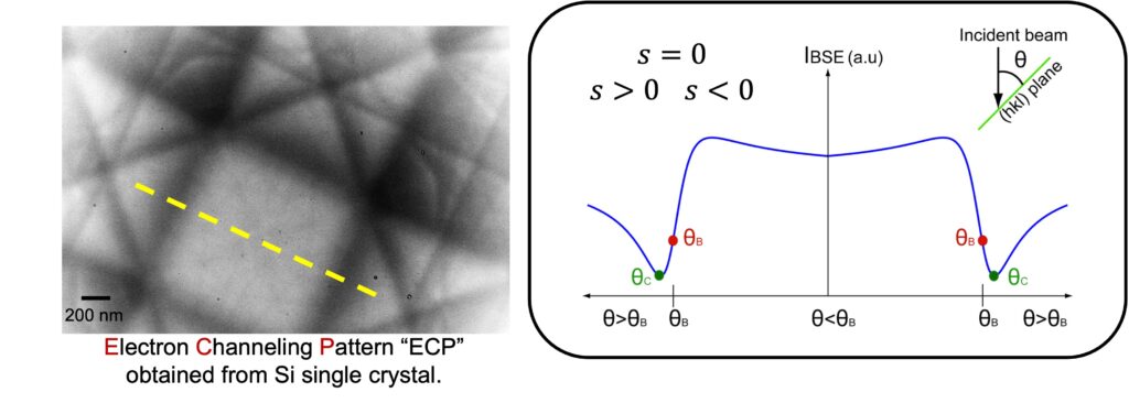
Electron Channeling Contrast Imaging (ECCI)
The characterization of crystalline defects extends beyond TEM experiments on thin foil samples. SEM can access diffraction contrast on bulk materials through electron channeling. Electron channeling occurs when electrons channel along crystal planes, creating paths for deeper penetration before scattering. As a result, different crystal orientations backscatter varying amounts of electrons, creating orientation contrast.
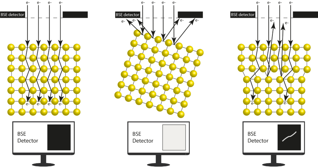
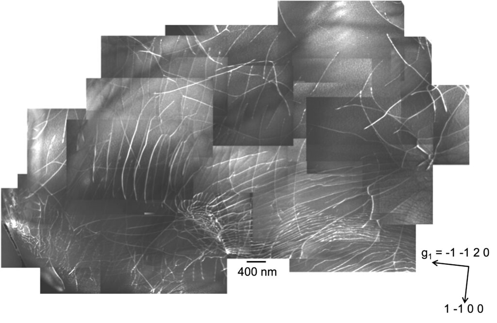
Electron Channeling Contrast Imaging (ECCI) is a non-destructive technique that allows for TEM-like diffraction contrast imaging of sub-surface defects (at a depth of approximately 100 nm) on centimeter-sized bulk specimens within an SEM. This is achieved by exploiting the fact that the yield of Backscattered Electrons (BSE) significantly varies depending on the crystal’s orientation relative to the incident electron beam, also known as the optic axis of the SEM.
The ability to characterize crystalline defects on a bulk sample in as much detail as TEM is possible due to extensive research on ECCI theory (Kriaa et al. 2017; Kriaa et al. 2019; Kriaa et al. 2021). Modern FEG-SEMs with adapted characteristics, such as high beam current mode, small beam convergence (quasi-parallel beam), and very small spot size, offer high imaging performance with high lateral resolutions (a few nanometers) and a good signal-to-noise ratio.
With these advancements, ECCI has matured as a technique for exploring new horizons. Recent studies have demonstrated its full potential in following the evolution of microstructures near interfaces, both before and after deformation (Habiyaremye et al. 2021). Additionally, to overcome the limitations of TEM for in-situ mechanical testing, macromechanical testing coupled with in-situ ECCI has been reported, highlighting its complementarity with simulations (Ben Haj Slama et al. 2021).
In conclusion, ECCI has emerged as a powerful tool for characterizing defects and investigating the evolution of deformation microstructures in various materials.